2010-09-10

Reducing a relay's control voltage on

Skip to modification
A relay is an electrically activated switch commonly used to control a higher auxilary voltage (like AC mains) with a smaller one (DC VCC).


The type I most commonly encounter are the general purpose 12VDC/5A 250VAC DPST found in PC power supplies and home electronics. These typically have control on/off voltages of 9.6VDC and 1.2VDC. However, it is possible to modify these to have a much lower DC on voltage.


This is an unsealed relay from either a 'broken' PSU or an old monitor; I'm not certain which but it doesn't matter. On the left you see the coil. The coil has a yoke wrapped around it. On top of the yoke is an armature that is held in one position by a spring. on the other end of the armature are contacts that form the switches.


When voltage is applied to the coil it forms a magnetic field that travels through the yoke and traps the armature to the coil. When the armature is drawn to the coil the contacts are closed together and a circuit is formed. When voltage is remove from the coil the spring brings the armature back to it's initial position, and the contacts are split open.

The control voltages of a relay can be changed by modifying the forces involved.
  1. {Von,Voff}*Fn/Fo
    Reducing the strength of the spring would reduce the amount of magnetic force required to move the armature.
  2. {Von,Voff}+Un-Uo
    Changing the deflection of the spring would reduce the amount of magnetic force required to move the armature.
  3. {Von,Voff}*originalpermability/newpermability
    Increasing the magnetic permeability of the yoke (mu) would reduce the reluctance of the magnetic circuit increasing the amount of magnetic force focused on the armature.
  4. {Von,Voff}-magnet
    Adding a magnet would preload the armature to connect with the coil.
  5. {Von,Voff}-battery
    Adding a battery in series would offset the voltages required.

The problems with these are:
  • Except for number 3 there is a risk that of going too far and having the arm stick in the closed position.
  • Numbers 4 and 5 has introduce a polarity sensitivity and complicates the circuitry required to compensate, and could lead to a latched mode of operation where a VCD less than 0V is required to switch off. Though this could have some applications...
  • Numbers 4 and 5 also introduce an element that will degrade over time and are not compatible with AC.
  • All of these risk reducing the control off voltage too far to be practical (ie: cope with a 'low' of 1VDC).

To only reduce the control on voltage a more thorough look at how the relay operates is needed.

{video: DMM 0,2,6,10(on),12,10,6,1(off)...}
The relay will remain 'off' until it has sufficient voltage to 'click' on (9VDC) and will remain on until it has insufficient voltage to stay on (1.2VDC).


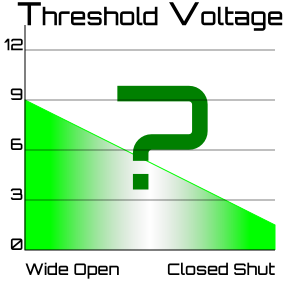
This indicates that from the initial open condition anything less than 9VDC is insuficient to 'turn on', but once it has closed anything more than 1.2VDC is enough to stay on. It can then be inferred that at some point after initial condition a voltage less than 9VDC is sufficient to hold on.

This stick is a precision instrument. Thanks Dustin.
This can be demonstrated by applying 2VDC and poking the armature with a stick. Repeated pokings will reveal that at a particular point of travel the arm will be caught by the coil and close the contacts. this is because as the arm travels the reluctance of the magnetic circuit is reduced as more lines of magnetic force are being caught by the armature and directed into the yoke.

{video: the stick in action}
Therefore if we were to pre-poke the armature we could reduce the control on voltage, and retain the same control off voltage since the other forces are not being changed.
Note: this will also reduce the effectiveness of the contacts in breaking the circuit since the 'open' position will be that much closer to closed.

Relay Modification
This is the a variation on the modification I did with the workshop, however with the abolishment of mandatory shop class so has too the ability to use a knife gone. I can no longer reccomend the use of a knife. If a knife is used, please be careful not to cut yourself, the coil inside the relay, the work surface, other tools, and other people. And if a knife is dropped, please don't catch it with your foot - adrenaline tends to turn a block into a punt- with predictible results.


Take an unsealed relay (identifiable by the plastic tab/notch at the bottom of the cover) and release the tabs holding the cover in place. A shim of plastic or paper may be used to prevent a tab from engag-ge?-g?-ee?-ing.


The cover has a finger that separates the two sets of contacts, and a void for the coil. Drill a small hole through the cover in the void directly over the armature, this will allow us to poke it through the cover.

Test fit the cover to make certain that the hole is over the armature and no other part. Adjust/widen if necessary.


Glue a nut to the hole. Make certain that the screw for the nut passes through the hole. This can be accomplished by puting the screw and the nut to the hole when you glue it. Be careful not to glue the screw yet.

While a screw could be put directly into the plastic cover it would be less secure and to be tapped out of its hole by the armature long after this has been forgotten about.

In this example I've used a 'nut' from a spare switch and duct tape to affix it to the relay. This is a bit of foil tape left over from my garage door repair, that has held through two winters without leaking or coming loose.

Replace the cover on the relay, and thread the screw into the nut.


Adjusting the relay can happen in one of two ways.
  1. Apply desired 'new' control voltage on to the coil and slowly tighten the screw until the relay closes (and make certain that it opens again at the desired control voltage off.)
  2. with out power to the coil tighten the screw until the contacts close then back off the screw until they open


The first method has the advantage of maximizing the contact separation when open, while the second minimizes the control voltage on.

In this example a minimum control voltage on of 2.7 VDC was achieved; lower values are not possible without modifying the contacts. The ability to extinguish sparks/arcing at this level is likely inadequate for practical application.

Glue the screw to keep this re-calibration.

Applications:
Reducing the VCC required for the control circuit allowing basic TTL control of an otherwise unsuitable relay.

Decreasing the response time of a relay for communications.

Running relays in series to reduce current draw from a control circuit in a kludge/fix.

Manually actuated relay as part of a power-return-control kludge.


Also, The parts for the SSD and cube have finally arived, but I am too busy to play with them. I won't be fixing the awful formatting in this post until I have the video from the workshop.

2010-08-21

New Toy, new project.

The head from a Curtis DVD8723.

I bought this on Craig's List and met the seller at Union Station. The ad originally indicated that there were no batteries, however it would seem that the seller installed a fresh pack of NI-MH cells, and was selling this because he is cleaning out his apartment, and would rather someone use it instead of throwing it out. This also explains the hand-made cable and other extras thrown in. (The DVD laser is not working, however the CD laser is, and it is a standard part if I decide to fix it later.)

Overall this is is excellent condition for my purposes, only one wire needed to be fixed (it was pierced by a screw), and only the pin configuration of the ports need to be determined. all are TRS 3.5mm or barrel connector, but 'S-video' and 'composite video' are the most curious. Composite seems to be carried by ring and tip (right channel), but using a TR connector produces the same results.

I plan on using this to build a portable IntelliVision since I have been wanting an IntelliVision again for years, and I figure it would look good in my portfolio.


This is the 25-in-1 IntelliVison Lives .comthat my dad (with some encouragement) has modified to accept an AC adaptor instead of gobbling up so many AA's every day. Sadly this is not an IntelliVision but is a Nintendo-on-a-Chip system made by TechnoSourcehk.com. Internally the glob of epoxy that is supposed to be covering the chip (Dunno which is the NOAC or the cartridge) isn't, exposing the extremely fragile wires. There is also no output filtering or amplification (except for what's on the chip). Between these two efectors of the many screens I've tried none are able to display the image correctly, there always instability and/or a lack of colour.

Fortunately running the signal through a video amplifier seems to cure the instability, and I have many video amplifiers. Unfortunately these are in VCR's, DVD players and tuners that are not very portable. I'm going to wait and see how 'good' the video out from a real IntelliVision is before I start making modifications.

I believe that I will need to scrounge for the parts I need for the cube and SSD locally. I doubt that my stuff will arrive.

2010-08-19

Calculator Battery

My calculator takes Alkaline batteries.
The MFG says LR44's but I know that LR6's will fit.

See.
I just had to drill a couple of holes, solder a cradle to the exposed lugs, add a couple of zipties and duct tape to hold things together.


The back cover especially.
No, the parts still haven't arrived, I fear that customs may have siezed them.

2010-08-11

Drop-in replacement PCB

for Nintendo Controller (model 004)

A dear friend of mine has passed away.
We'd often made potentially career ending bets that I'd do some incredible thing (instead of the conservative assigned duty) and my friend would keep admin off of me long enough for me to pull it off.
I've felt fustrated not being able to celebrate completion of the last bet, esp. with ideas for the next.

But this has given me food for thought whilst I wait for parts to arrive for my other projects. I've made many similar (though less damning) bets with other friends, and I'd hate to see them gone before I've finished.


This PCB is for one of my friends who is a NES freak.

This (surviving) friend has [reportedly 1 dozen of the] 'original' controllers that are so badly worn that even the repeated application of a chemtronics.comrubber key repair kit does no good since it the PCB and/or the plastic caps that have completely worn away.

For a laptop I bet that I would produce a replacement controller from a broken NES controller. This controller would either precisely match the original and use the same case, or it would be clever and be far more ergonomically correct.

I got the laptop within a week but my friend has never sent me a broken controller. I have never had a NES myself. And years later, I've now decided to search the internet and see if I can find the information I need to make a replacement PCB for the NES controler.


Search results:
NES ControllerI first tried working from the photo on slagcoin.com but was disappointed by the insufficient 0.05" resolution I'd achieved in the result. I believe that I miscalculated the trapezoidal transformation.

Rather than repeat the process I searched again using a number of premutations and eventually found an x-ray on flickr.com that was perfect; No distortion, square and true. All I had to do was measure and scale.

The result:
  • A drop in replacement PCB that is within 0.025" of the original model-004 (rev.11) NES controller PCB using the original components.
  • Tact (10xx) switches have been drawn to allow replacement in controllers where the button/key caps have worn out.
  • Combs instead of panels to improve the useful life of the membrane switch, and minimize alignment issues.
  • The header has been changed from rev.11's {GND,CLK} to rev.5's {GND,VCC}.
  • 'Umbrellas' have been drawn under the resistors to prevent the ground mask from raining on the use of printed resistors.

Since I have no 4021 I am unable to build this circuit today (without ordering parts). The CMOS 40xx series of IC has been displaced by the TTL 74xx series. If I needed to I would need to make an extra a 74xx design based on what parts I have on hand. This extra design would also make sense if my friend has lost the original PCB or wants to make a spare.

A 74xx redesign:
  • The original printed M5923 resistors have been replaced with common throughhole 207's. These are grouped where the original 4021 was for stylistic reasons.
  • The original 4021 has been replaced with a surface-mount 74HC165 (since that is what I have on hand).
  • A transistor replaces the header and inverts P/S to output SH/LD because the 74165 loads on high unlike the 4012 that loads on low. (see nxp.com datasheets HEF4021B.pdf, 74HCt165)
  • All resistors can be 10k (though not optimum for the transistor inverter/NOT gate).

Modifications not implemented:
  • 40xx instead of 10xx switch because the larger 40xx would break compatibility with the original layout unless I were to intersect the pads, which would then make assembly very difficult.
  • Use of a resistor array instead of discrete components because I'd be inclined to use a single surface mount IC, and evidently a pitch of 0.012" is too small for most people to assemble by hand.
  • LEDs that are activated by button presses because I do not have a NES to test if this works.
  • Turbo/pulser because adding a single IC programmible division counter or frequency generator w/ selector switches would require my (not an electronics hobyist) friend to handle too many pieces, and would require modification of the original case.


2010-08-08

Fixya. Fixed/Neutered.

I am a user on Fixya.com.

While they have 'fixed' the problem of hidden formatting consuming space in posts, as encountered here. They have done so by brutally sanitizing the HTML to the point where it will delete any specaly formatted content, often losing the critical distinction between A and A or B and B.

Sorry about asking to be contacted here, but I don't want to expose my current e-mail on a help forum and it is no longer possible for me to embed it to be visible to only the intended recipient on Fixya now.

2010-07-20

`ell, only one letter off.

A few years ago I canceled my spare Bell internet account because they would nolonger allow me to suspend it and resumed billing me unannounced, would not allow me to move the email to another acitve account, and would not allow me to only pay for hosting.

$25/mo for an email service that deletes my email without warning was a bit steep and I told them then to close the account.

I figured that after a couple of years the name would be released and I would be able to reopen it with my current one. This is what happened:

System
Welcome Darren {### ####}.
System
Connecting to server. Please wait...
System
Connection with server established. Please wait...
System
Balaji has joined this session!
System
Connected with Balaji
Balaji
Hi Darren {### ####}, welcome to Bell Internet Services, my name is Balaji. By looking at the option you have selected, I see that you have questions regarding your account, how may I assist you with this?
You
I am tryign to move my old emailaddress again.
You
IN 2007 I canceled a redundant account when maintaining it became too expensive.
You
I was unable to associate my original username/email with my current account.
Balaji
Sure, I'll be glad to assist you in moving your E-mail address Darren.
You
I need to do so now to consolidate my identity.
You
thankyou.
Balaji
Welcome.
Balaji
Could you give me a couple of minutes so that I'll get the information for you.
You
yes.
Balaji
Thank you for being on line.
Balaji
Once the account is terminated, the E-mail account associated with the account is also terminated.
You
However the user handle was not. I am unable to use "{####_###}"
Balaji
I apologize for the inconvenience caused to you.
You
The account { b1{######} / {#######} } still appear valid to one bill too, though I have forgotten the password.
Balaji
The E-mail also comes with the account. Once the account is terminated you can't access your E-mail Darren.
You
I never expected to; however the fact that the handle was not released is actually a good thing. It means that someone else cannot assume my identiy as easily.
Balaji
I am sorry for that.
You
Don't be, it was some major oversight that there is not an extablished proceedure for moving e-mail addresses between accounts.
Balaji
The E-mail also comes with the account when you have subscribed with Bell. Once the account is terminated you can't access your E-mail Darren.
You
... By which I mean that I have multiple bell accounts, but when I moved back to my mother's there was no mechanism by which we could keep both email's without paying full price for both accounts.
Balaji
May I have the b1 number of the active Internet service?
You
b1{######}
Balaji
Thank you.
Balaji
There is no possibility to have the {####_###}@sympatico.ca , because you account (b1{######} ) has been terminated.
You
...
You
There is no means by which the email from the terminated account can be associated with the active one?
Balaji
I have checked the information Darren you can't associate the active account. As your account is Terminated.
You
So since December of 2007 all bell customers who moved in together, got married, merged businesses, combined offices, ect. They all have had to either pay an obscene amount of money for 'just the email' or give up that identity, and the professional/personal connections therein?
Balaji
here is no possibility to have the {####_###}@sympatico.ca , because you account (b1{######} ) has been terminated.
You
Yes?
Balaji
The E-mail also comes with the account. Once the account is terminated you can't access your E-mail Darren.
You
If i were to pay to reactivate the account, would the email address then be portable?
Balaji
I do understand Darren. Unfortunately it is not possible to reactivate the account once it is terminated.
Balaji
Darren, I do understand your concern, Email is a service provided by Bell together with Internet service, and all email accounts are connected with their internet accounts.
Balaji
We cannot provide email service alone to any customer, The internet account once terminated cannot be reactivated.
Balaji
Darren, you can try to create the {####_###} email address with gmail, yahoo or hotmail.
Balaji
I appreciate your understanding in this regard.
You
THe problem is that I associated my {bank}, {portfolio} and other professional accounts with this address becasue at teh time I belived that this was safe. When emails started disappearing (becasue my ### stole the acount information and some idiot kept resettting the password for ###) I moved most things to another service, however these two accounts are permanently associated with this address unless I can countersign an email from them.
You
I understand that there is no established method for remeding this currently and I will pursue another avenue for resolution.
Balaji
I'm really sorry and I apologize for the current situation.
You
Out of morbid curiousity; Does Bell currently have a mechanism by which email-addresses be moved from active accounts can ?
Balaji
Darren, I can understand your need for the email address, however email addresses cannot be transferred to different address.
You
thank you for your efforts.
Balaji
You are welcome.
Balaji
Is there anything else that I can do for you?
You
I will be reposting this chatlog, would you like to have your screen name redacted?
Balaji
Darren, I have provided the information to you based on the actual policies of Bell.
You
Then that is all. Thankyou again.


So eventhough they know it's me, they still have the account on record, and will never use that username/email for any other purpose they will not even sell me my email and are telling me to go away.

The address cannot be moved from any account to another. The original address cannot be removed from the first account. And the account cannot be reopened for a couple of weeks for any amount of money.

It would seem that Bell is only interested in customers who are in a rut and are unprepared for / have no idea why anybody else would be on the internet.

In a nutshell;
if your situation changes for better or worse and you find yourself sharing your line with another Bell subscriber, Bell is telling you that you both would have been better off using Hotmail from the start unless you have the money to pay for two broadband connections, since Bell nolonger sells 'only email' or 'dial-up' anymore.

I am defintely going to see if I can't get bell to fix this.

2010-07-19

'... ,' it may not be golden,

but it definitely stands out.


Another one of my duct-tape repairs.

The clic mouse nub has been loose for a while; about a week ago it got caught under the /'b/' key while I was typing and I managed to break the tabs that hold it on its cradle, rendering it useless.

Rather than waste an entire keyboard for one key or break the membrane by pressing on it directly; I decided to wrap the key to its cradle with duct tape.

It has held up fairly well, though I have to occasionally retype things where /'b/' has not turned out as expected.

2010-07-17

Card shuffle.


This is an alternative Clone t`engineering design using the NV SRAM. It is approximately half the size of the original though most of the space is wasted. It uses less than half the components though only the SRAM array and power circuitry has been concatenated. And it is a quarter of the cost though it still is using DIP packaging. And all of this without a radical departure from B. Yahya's original design! (Yay progress!)

A casual glance at the schematic shows I have opted not to wire the address lines in normal order; this shuffling of the address lines creates new problems when programming this board. Including having to make an adapter for your logic analyser/bus sniffer if it has a hardwired hat. Needing to store the ROM image in that peculiar byte order. Debugging if it was a programming or image processing error causing a software malfunction. Having your most fastidious colleagues complain* that you badly screwed up the design of the project citing the prefered logical order for the ICs in question, shouting that it can't possibly work.

However, this approach has strong advantages over fixed logical ordering. First: it eliminates the need for vias to satisfy an artifical ordering requirement. Second: if a competitor dumps the ROM without reverse engineering the board the image will appear corrupted. Third: Gives you something to write about. Fourth: the satisfaction of saying "I told you it would work" to you colleagues after a job well done.

Shuffling, not to be confused with stacking:
VPP27256VDD
A12A14
A7A13
A6A8
A5A9
A4A11
A3OE
A2A10
A1CE
A0D7
D0D6
D1D5
D2D4
VSSD3
VPPmutantVDD
A0A1
A2A13
A3A4
A14A5
A6A7
A8OE
A9A10
A11CE
A12D7
D0D6
D1D5
D2D4
VSSD3
Difficult hardware, hard software.


From the above we see that the address line order {A0-20} is now
{12,11,9,8,6,14,3,2,4,5,10,7,0,13,1}. We can reason that the value stored in 0x0000 is now read from 0x0000, but the value in 0x0001 is now read from 0x0004, 0x0002 is now read from 0x0001, 0x0004 from 0x01000, etc.

The ROM chip is read externally out of order while internally the image is stored sequentially {00, 01, 02...}. The image must be distorted/mutated to match the read order else it won't be read back correctly. One method is to build an adapter for our programmer that would shuffle the address lines for us; however some ROMs do not behave well if written to non-sequentially and every design would require a different adapter. Making this a physical hardware adapter would either exaust our resources, or require constant reconfiguration, leading to inevitable calamity from loose/misplaced connections.

//Advanced Hex Editor script, does not work!

//address[write]=2^[read]
a[0]=2^12;
a[1]=2^11;
a[2]=2^9;
a[3]=2^8;
a[4]=2^6;
a[5]=2^14;
a[6]=2^3;
a[7]=2^2;
a[8]=2^4;
a[9]=2^5;
a[10]=2^10;
a[11]=2^7;
a[12]=2^0;
a[13]=2^13;
a[14]=2^1;
// base betweeen iterations, avoids an inner loop/summation.
B[0]=0;
B[14]=0;
ii=0; //because I don't feel like calculating an index for a sequential read.
D[0]=0; //Image holder.
D[32767]=0;

for(i[0]=0;i[0]<a[0];i[0]+=a[0])
 {B[0]=i[0];
 for(i[1]=0;i[1]<a[1];i[1]+=a[1])
  {B[1]=B[0]+i[1];
  for(i[2]=0;i[2]<a[2];i[2]+=a[2])
   {B[2]=B[1]+i[2];
   for(i[3]=0;i[3]<a[3];i[3]+=a[3])
    {B[3]=B[2]+i[3];
    for(i[4]=0;i[4]<a[4];i[4]+=a[4])
     {B[4]=B[3]+i[4];
     for(i[5]=0;i[5]<a[5];i[5]+=a[5])
      {B[5]=B[4]+i[5];
      for(i[6]=0;i[6]<a[6];i[6]+=a[6])
       {B[6]=B[5]+i[6];
       for(i[7]=0;i[7]<a[7];i[7]+=a[7])
        {B[7]=B[6]+i[7];
        for(i[8]=0;i[8]<a[8];i[8]+=a[8])
         {B[8]=B[7]+i[8];
         for(i[9]=0;i[9]<a[9];i[9]+=a[9])
          {B[9]=B[8]+i[9];
          for(i[10]=0;i[10]<a[10];i[10]+=a[10])
           {B[10]=B[9]+i[10];
           for(i[11]=0;i[11]<a[11];i[11]+=a[11])
            {B[11]=B[10]+i[11];
            for(i[12]=0;i[12]<a[12];i[12]+=a[12])
             {B[12]=B[11]+i[12];
             for(i[13]=0;i[13]<a[13];i[13]+=a[13])
              {B[13]=B[12]+i[13];
              for(i[14]=0;i[14]<a[14];i[14]+=a[14])
               {B[14]=B[13]+i[14];
                D[ii]=get1u(B[14]); //Gets 1-byte unsigned value at offset
                ii+=1;
               }
              }
             }
            }
           }
          }
         }
        }
       }
      }
     }
    }
   }
  }
 }
for(ii=0;ii<32767;ii+=1)
 {set1u(ii,D[ii]);}//overwrite original.


The above script uses nested loops to represent each bit of the address line. It sequentially reads the bit and stores it in the correct 'shuffled' location.

I acknowledge that there are some operands not represented in Kahei or C that would allow for a more efficient program. And that using a matrix would be far faster and more efficient. However such an approach would be far less flexible and difficult to understand. And the effort required to build one I cannot justify especially for a program that would normally only be used once. But I am a hardware guy, an expert programmer may not have the same difficulty.


Before I get complaints that I am being unfair to the original designer let me point out that there has been 18 years of technological development since it was created; B. Yahya had the courage (and ethic) to publish this design at a time when many companies were terrified to; The original design itself was so well done that unaltered it is possible, though not commercially viable to produce it today; And the autorouter jab is fair game as vias should not be inside an array, except where lines cannot run parallel or for thermal reasons; Also, the original was a success; wasn't it?

2010-07-15

Clone t`engineering

Part 3: continued from Cloning for fun or profit

Copying this card is not enough, were we to make a profitable version it would need to be cheaper, and if we were reviving this product its replacement will need to be better.

To pursue both of these an understanding of the originals function, and how it functions is essential.

Schematic of the original


A quick survey of the original we see:

ICs1-1662_1024128K × 8 Static RAM
IC 1727_256256 K (32K × 8) CMOS EPROM
IC 1874_5738-bit D latch BUS DRIVER; 3-state
IC 1974_5908-bit BINARY COUNTER
with output register
IC 2074_245Octal BUS TRANSCEIVER
ICs21,2274_6888-bit MAGNITUDE/IDENTITY COMPARATOR
IC 2374_1544-line to 16-line data SELECTOR/MULTIPLEXER
ICs24,2574_5748-bit D type FLIP FLOP bus driver; 3-state
IC 2674_1383-line to 8-line DECODER/DEMULTIPLEXER
IC 27MAX690WATCHDOG / Supervisory Circuit
IC 2874_08Quad 2-input AND gate
IC 2974_32Quadruple 2-input OR


8-BIT IBM/ISA Card Edge

The most ovbious parts to save to save money on are ICs1-16.

The cheapest 0.1" pitch DIP package with 128K×8 (at the time of this article) is Digikey.com:BQ4013YMA that hit our 4.5-5.5 VCC sweet spot, is Non-Volatile (NV) SRAM eliminating the need for IC 27 and a battery, and at $25.94 per IC, it would cost $415.04 before applying the new HST and Eco taxes for enough capacity.

If we were to move to a surface mount 0.05" pitch SOP package such as the Digikey.com:IS62C1024AL with 2.0 V data retention threshold and the same VCC, it would cost $4.23 per IC, $67.68 for all sixteen.

However;
Buying Sixteen 128K×8 ICs is silly when we could subsititute a single 2048×8 IC for ICs1-16 and IC 23. Reducing our component count and board size by more than half, while remaining software compatible with the original.

ICs1-16 can only accept address lines 0-16, but each can be individually addressed, therefore IC 23 decodes address lines 17-20 and individually addresses ICs1-16. If there is only one SRAM IC then a decoder is unnecessary and can be eliminated while leaving the original software completely unaltered.


Illustration of difference in complexity between using a single surface mount IC w/ an unused or gate from the original, and the orignial's 17 ICs. Additional power circuitry required.

A single 2048K×8 DIP such as the Digikey:BQ4017M would set us back $107.84. Or a 0.0315" pitch TSOP like the $44.44 Digikey:CY7C1069AV33. Both of which are a king's ransom compared to a $7.22 Digikey:NAND512W3A2DN6E 512MB Flash 48-TSOP-II, or a modest $1.07 Digikey:SST25VF040B 4MB Flash 8-SOIC, both of which would require the use of different hardware and software.

I should be able to learn enough from reverse engineering this hardware to better understand how it works and where we might find areas of improvement.


When (IOSel=0 and Reset=0) IC26 decodes (AD0-2,CO,RST)
When IC28D(IORd=1 and IOWr=1) if [(SA3-9 is (ID0,ID1,00011)) and (AEN=1)] then IC22 sets (IOSel=0)
When (MemRD=0) if [(SA13-19 is 0011011) and (Reset=0)] then IC21 sets (MemSel=0)

When (MelSel=0) IC17 decodes (D0-7) by (SA0-12,ID0,ID1)
When IC28B(MemSel=0 OR IOSel=0)
IC28C will turn off D1 sinking current to drive LED.
Also, If (IORd=1 and MemRd=1) IC20 loads D0-7 onto SD0-7
ElseIf (IORd=0 OR MemRd=0) IC20 loads SD0-7 onto D0-7

When (AD0=0 and IOWR=0) IC29A sets WE=0, else WE=1

When (AD0=0 and CS=0) IC23 decodes A17-20 and activates the correct CS1-16 for the SRAM array, else they are all disabled.

When AD0 rises IC19 increments its register;
When system CLK rises IC19 outputs its register to A0-7 // if system CLK does not cycle after AD0 then an address is skipped!
When RST=0 IC19 resets its register

When CO=0 IC18 loads K1 onto D0-7 // external input/jumper config

When AD1 rises D0-7 is loaded onto A8-15
When AD2 rises
D0-4 is loaded onto A16-20
D5 is loaded onto CS
D6-7 is loaded for no apparent reason // load balancing for lower quality components? to make routing the wires more difficult? To avoid colleagues complaining about not having all lines of the databus connected?

JA3-4 pull ID0-1 to 0 when set

The SSD's address without jumpers is 318H, with JA3 is 10H, JA4 is 306H, JA3,4:300H .

IC21
IC28
IC26

D 8-9 3-F 0-1 0-F
ID 1101100___11000xxyyy
SA 3210fedcba9876543210
0x300

b 1100000000
0x318

b 1100011000


Assuming both jumpers are set we have a IO base address (BA) of 0x300, then
BA+0 is AD0
BA+1 is CO
BA+2:RST
BA+3:AD1
BA+4:AD2
(+5,+6,+7)

An IOread to 0x__302 would activate CO and IC18 would load K1 onto the system databus via IC20.
An IOwrite to 0x__302 would also activate C0, but, but IC20 would change direction and 'fight' it potentially damaging the chips - This would be bad.
Make a note that 0x__302 should be treated as read only,
Similarly any read or write to 0x__304 where bit D5 is set, activating CS, should not be followed by an instruction that makes use of the SSD's databus except to access SRAM- this would also be bad.

Our ROM base address is 0xD8___.

A quick peek into the image reveals
seg000:002Adb'Yatronic Silicon-Disk V2.0 (c) 1992'
seg000:004Ddb0
...
seg000:6800 db '                '
seg000:6810 db ' COPYRIGHT Uitg.'
seg000:6820 db ' ELEKTUUR B.V.  '
seg000:6830 db '      BEEK      '
seg000:6840 db ' The Netherlands'
seg000:6850 db '      1994      '
seg000:6860 db '                '
seg000:6870 db 'Author: B. Yahya'
seg000:6880 db '                '


Disassembly to follow.


2010-07-12

Eazy, like riding a bike.

The EZ-USB board last mentioned on this blog in Yeah! was built a while ago. Even used some of the board art as the background to this blog. But I did not post the build logs because I must have been clicking the wrong button all along.

I'll summarize the build here:

Oddly the most arguious part of this build was getting the PCB made. There was a miscommunication and I misunderstood that the PCB design would be sent out after my boss 'did something' to the Eagle files. That never happened, instead when I went to collect the PCB I received a blank piece of photo-sensitive board and a (discount brand) transparency sheet.

In the time since I last made a board by photoengraving we had installed a new experimental etching process. A year ago we diped the boards in heated baths of feric chloride (etchant) with an array of aquarium air pumps to provide circulation. Now we had a metal cage that holds the blank PCB in a small container with twice as many aquarium pumps blasting the etchant onto the PCB, no heater. This is partly because disgruntled jokers kept bypassing the automatic shutoff and leaving it on over the weekend, but mostly because when the etchant is opaque this still will etch a board in a couple of minutes.

My lack of familiarity with the new arrangement meant that it once I had the pattern printed onto the transparency (which was unexpectedly difficult due to network problems) it took four attempts to get a useable board.

Fail #1: hot seat.
It seemed to have etched nicely when I checked it after three minutes, however when I did extract it there was a long scratch across the board that cut through rows of wires. These had to be bridged using wires, dozens of them.

There were dozens of vias too since the original design called for the lines to be brought out in signal rather than pin. These were connected using wires, dozens of them.

The vias that would be concealed by the main IC would also have allowed easy rework if the IC was off its mark. These also are to meet for specific power requirements. The new plan called for the 24 gauge wire to form a platform under the IC and bending the pins down to the board, a baker's-dozen wires, and a hundred pins.

I'd done this with a 20-SOP (0.05") and even a 48-TSOP (0.02") before and figured that it would work with a TQFP-100 (0.02"). After many attempts I could not get the vertical pins onto their pads no matter how many times I tried and I figured that the chip must be riding up at an angle on these wires.

After disturbing much of the fancy repair work I'd done earlier it seemed likely that the IC would not have enjoyed this much heat so etching another board and using 30 gauge FFC instead seemed more reasonible than continuing.

Fail #2: repeat.
Being very careful not to scratch the mask I photo-developed another board and then used a Sharpie 'industrial ink' pen to draw in the details that didn't turn out, put it into the etchant and watched.

After a few seconds it became clear that the board was not being etched evenly, and I very gingerly repositioned the board when the definition of the traces were clear in one patch, but not the rest of the board.

Eventually it became clear that part of the photo-mask was eroding but other areas were not etching. This was probably due to a combination of uneven circulation of the etchant and contamination of the board. (my colleagues were eating fried chicken and also making PCBs for their own projects) TO fix this I tried to cut the copper between traces w/ my knife and return the PCB to the etchant. This did not result in the copper being removed after a couple of minutes. So I removed the board to try again, at which point a bit of the vynil I had used to hold the board to the cage brushed against it and removed part of the normally acid proof mask.

Fail #3: cleaner is better?
After decling to go to the pub with my friends/coleagues for lunch (which I regret) I tried again.

This time thoroughly cleaning all of the equipment and replacing the photo-developer solution, to eliminate contamination. Collecting a fresh blank PCB to avoid mask voids where air has leaked in and eaten it away. Over exposing the board to make absolutely certain that not even an invisible trace of the mask remained. And finally resolving not to handle the board once it was in the etchant.

This did not work.

While I was working through the chicken my friends had left me the board was buffeted against its cage and recieved many scratches. And the over exposure caused many defects. All of which would require hundreds of wire bridges to repair.

Fail #2: the sequel
Not anticipating any greater success with the current pattern, I went ahead and tried to repair these boards and if another PCB is to be made in the same manner than a new design would be used, one that is single sided and not 'consumer ready'.

I drilled the hundreds of vias/pads by hand before heading home where I pre-soldiered the entire surface of both boards to eliminate any small break. Used the CAD files and my knife to carved every single line that did not etch from Fail #2 out of the copper cladding. Used a desklamp and a marker to highlight the dozens of breaks in the pattern.

Fail #0:
Back at work the next day I tinned a fresh chip, and positioned it on Fail #1;

It did not fit.

I did check the fit on a plain piece of paper; but the transparency was clearly out of scale when I lay it ontop. Want to know how was this was possible?

Remember the printing problems?

We have a mix of Win9x, Win2k, Mac and Linux machines, and everyone outright owns their own machine in addition to the pool of machines provided. We also for baffling reasons don't use printing permissions, so often times someone in one department will try printing to the first printer they see on the network, instead of the one they are sitting next to. And when that doesn't work they try printing again. Then when that fails they try another printer at random. And when that fails they try the first one again. ...

Now this wouldn't be an issue if we didn't have seven printers in on the main print server workgroup and another fourty in various offices. My lab's printer is the first one on the list so it is often out of toner and paper, or getting stuck when someone ques to print A4 and it only has letter and A3. To combat this IT has set the print server to always override print-settings to use HP's 'econo-mode' if a user prints twice to the same printer within a 30 minute window.


Econo-mode itself is actually quite clever. It applies a gradient to dark areas so that the edges that the human eye follows are clear but less toner is used in the middle. And the page is scaled vertically by 5-15% depending on the amount of toner used on each line, tightening line spacing and saving even more toner. All of which does not negatively affect human readable text and graphics.

But my work is technical. A 5% distortion is enough to put a sliding rule graph out by an entire order of magnitude. And even regular scaling to a PCB prevents pieces from mating, printed component to be incorrect values, IC pins sitting onto the wrong pads, header pins not fitting without breaking.

At this point I cursed and redesigned the board and stayed late to finish building the board.

Success from failure:it just never ends.
Redesigning this board a fifth time has allowed me new insight to its design. This iteration brought the board to approximately the size of a floppy disk, and there was no real need for it to be breadboard sized, and the whole peripheral plan was a bit half-baked. As a 3.25" double sided board it would have sufficient space to bring two rs232 transceivers and keep the extra leds and buttons. I've never seen a user plus the original into a breadboard and build their circuit next to it anyways, it's always three boards, one for each edge and one for the circuit.
Now it's one plus the double sided 3.25".

The tie in: product placement.
The SSD mentioned on this blog in Cloning for fun or profit can be reduced to four chips, this SoaC, voltage-level converter, power and SRAM. And the sweet part is that now the medium for loading/unloading data from the XT/AT can be a USB cable, and users can expand the capabilities of this card using software.

There are a few more posts to summarize about acually programming this chip, but I will continue that in a later post.

2010-07-08

Cloning for fun or profit

Cloning a piece of hardware is an excelent way to learn about how it is designed, and how it works. This is often viewed as a seedy trade inwhich people bastardise the hard-work of honest engineers and other designers to produce the same product without the overhead cost of design and marketing.

Unfortunately in my experience design documentation is almost always lost and the only way to recover (or sometime resume production of) a product is to clone it and there is little discussion on techiques for achieving this.

Generally when I 'clone' a product, I build an exact replica (in so far as component layout and electrical connections). Then I go looking for what can be made cheaper. Then better. Then the maintence cycle begins.

I like to use high-resolution photography and logic probes to start with; however grainy photographed pages from a foreign trade magazine from a random website is more than enough to clone a product and start development.

Take for example the Solid State Diskdrive for the IBM XT featured on K. Giannopoulos' website (microwave.gr:Build your own Vintage PC-XT Computer). From these massive bitmaps, and roms we can produce plans for a clone and then some.

Step 1: Preparing the reference material
To obtain the reference board art start by tracing the bitmaps with Inkscape. This allows evaluation the quality of the reference material and gives me a reference for the wiring of the first clone.

Next using the outside corners as reference points calculate how much to rotate these layers to align their edges horizontally.

Top layer
  • (1463.789,5.971)
    0.233716199°
  • (1468.760,3.486)
    0.135987303°
  • 0.184851751°

Bottom layer
  • (1464.944,2.279)
    0.089134448°
  • (1468.780,9.950)
    0.388134564°
  • 0.238634506°


Okay;
In this example because the bottom layer is clearly out of square as the angle does not match, this could be because of perspective, a transform can fix that if it is flat. There is also noticable distortion bacause the pages were not pressed flat when the picture was taken, but maybe I will get lucky and manage to align it anyways.

Nope.


The red top layer does not completely align with the blue bottom layer. There are also a number of 'broken' traces where the line did not render very well. Even if this image was rescaled a pcb made precisely to this image the pcb would require significant repairs where the components do not fit, where the layers do not connect and where the wires are disconnected. Fixing this would be quite difficult.

If it were in alignment we could then replace the polygons with wires and convert this into gerber format using a script. But it's not so I will be drafting the board art manually. Fortunately this website also posted a schematic and parts list.


Step 2: Using the reference material.
Add all of the parts necessary to a new Eagle schematic. I found that I needed to add two 'new' comonents to the library: the three lead capacitor and the DIP32 RAM.

Working from one corner to the other recreate populate the schematic and board with approximately the same layout. Once populated wire the schematic and board as close to the original as is practical. The reference art can be coloured to track progress and distinguish different signals easier.

I think lavender is a fine colour for the data bus.


While I was doing this I made a few interesting discoveries: most significantly was the omission of CLK from the cardedge to IC19 on the original schematic, without this a clone card made only from the schematic would not work.

The secret CLK.


The Address and Data lines were also shuffled around by the orignal designer to help with board layout. This is good since even with the bits shuffled around each address is still unique and the data (provided it is always stored in the same order) will still read back correctly.
As evidenced by the vias inside the array of memorychips the previous designer got bored and used the autorouter resulting in some spectacularly stupid wiring.
I've duplicated most of the 'stupid' so that my colleagues will not harass me about differing from the original "too much", though while linking the data and address lines from the memory chips I made a hash of it since I intend to design that out entirely.

And here is the result of eleven hours of unpaid work: a clone of the original board, minus some stupid, plus some sloppyness when I got bored.


Now that we have a hardware/software compatible clone we can make it cheaper by substituting components.

Part3: to be continued


Note: I was unable to upload the PDF, SVG, brd, sch and lbr files I had intended to illustrate this post with. I am also disinclined to seekout a file host for these if nobody asks for them.

Edit: I have been contacted, links to follow.

Edit: Build your own Vintage PC-XT Computer files are availble in the Solid state disk section.

2010-07-03

Re: Broken wire in collector cell

I am posting this here because of a post length limit on Fixya.com.

This happened to me.
If the tiny wire touches another layer in the collector cell it will short.

You could remove the wire, however that would reduce the effectiveness of your cleaner and may void your warranty.

This is how I repaired my 'broken' cell. Only attempt this if you are very good with a pair of pliers and do not mind voiding the warranty.
  • Cell disassembly
    1. remove the collector cell from the air purifier

    2. Separate the charcoal filter and dust screen

    3. standing the cell on its edge press firmly down on the edge of the metal contact and release the tab holding it in place
      • The metal should lift from the plastic tab without any resistance

    4. This should expose an electrical contact rail with metal tabs folded up/down onto it. Lift and straiten these tabs
      • Care should be taken not to break these as these are what hold the cell together mechanically and electrically

    5. {Repeat for all four contacts}

    6. Slide the ends off of the filter and carefully remove the center combs/clips that maintain the spacing between the layers of the cell
      • These are held in place by plastic tabs that are rigid. These tabs will not separate easily but will break if they are bent too far.

  • Layer Disassembly
    1. Lift the metal tabs that hold the wire in place. This is easiest by pushing the tab through the 'bottom'
      • In all three of my units the metal wire was wrapped around the tab before being crimped in place

    2. Unwind the wire from the tabs and set it across the tabs

    3. Crimp one end of the wire in the end tab by pressing the tab flat (back into its hole) over the wire. If you have two pieces of wire use tabs at opposite ends of the layer
      • Flatness is important, as any bump will create a short gap at which the voltage can leak/arc more easily

    4. Bring the loose ends to the center tab tightly and crimp those in place, being careful to wrap up an ends that could produce a spark-gap with a neighboring layer

    5. Press all of the tabs securely and trim any stray bits that could produce a short or a spark

  • Suggested Cell assembly

    1. Flatten the end tabs of each layer that they can fit into the slots in the caps more easily

    2. making certain that the layers are orientated correctly and in the right order slot each one into an end cap

    3. Check that these are in the correct order!
      • Are the layers {flat, wire, flat, wire, flat, wire, flat, wire, flat}?

      • Is the label on the outside?

      • Is the label on the top, where the dust screen is inserted from?

      • Does the Front arrow on the label point to the dust screen?

      • Are all of the wires infront?

    4. Once you have gotten that right make certain that the contact rail is in place on the end of the cap and fold the tabs up/down securing the layers

    5. Replace the plastic combs/clips from the center of the filter
      • this is easiest one layer at a time

    6. Install the opposite end cap and secure those tabs

    7. Replace all four metal contacts

Note:
Oreck replaced my unit in full knowledge of my repair however, this was a gratuitous act outside of warranty. Do not expect a replacement if your repair is unsuccessful or detected.

Edit:
It has been suggested that it may not be necessary to remove the layer from the cell. I havent had to try that but will in the unlikely event that I have another wire break.

EDIT:
Fixya fix this.

2010-06-05

What?


Adding symbol GND to F09-S would exceed the minimum number of pads (11) availble in package variant V


This is a device I copied directly from Eagle 5.7.0's library (con-subd.lbr) because in my design only one of the two shield lugs were being wired. I was only conecting to 10/11 pads, but adding annother GND symbol increasing the symbol count to 11 actually exceeded the pad limit of 11.


The connect window shows that there are infact 11 pins already defined, including G1 and G2. Typing show G1 in the command line is unsuccessful, therefore these pins must be defined within a symbol.


A look at the symbol (GND.sym) appears to illustrate a single pin, right clicking and selecting properties reveals G1, a wire and a circle. G2 must be nearby, and show G2 in the command line reveals that it is hidden under G1, backwards!


So in the schematic editor by using the wire tool and clicking on the GND symbol only the top pin was engaged. Had I run Eagle's Electrical Rule Check it would have produced a warning that would have confused me and prompted the same response.


The workaround:

This is a common symbol in Eagle's library, let's hope that 5.9.0 has it documented.

EDIT: typo, G2 and G1 transposed.