2010-07-08

Cloning for fun or profit

Cloning a piece of hardware is an excelent way to learn about how it is designed, and how it works. This is often viewed as a seedy trade inwhich people bastardise the hard-work of honest engineers and other designers to produce the same product without the overhead cost of design and marketing.

Unfortunately in my experience design documentation is almost always lost and the only way to recover (or sometime resume production of) a product is to clone it and there is little discussion on techiques for achieving this.

Generally when I 'clone' a product, I build an exact replica (in so far as component layout and electrical connections). Then I go looking for what can be made cheaper. Then better. Then the maintence cycle begins.

I like to use high-resolution photography and logic probes to start with; however grainy photographed pages from a foreign trade magazine from a random website is more than enough to clone a product and start development.

Take for example the Solid State Diskdrive for the IBM XT featured on K. Giannopoulos' website (microwave.gr:Build your own Vintage PC-XT Computer). From these massive bitmaps, and roms we can produce plans for a clone and then some.

Step 1: Preparing the reference material
To obtain the reference board art start by tracing the bitmaps with Inkscape. This allows evaluation the quality of the reference material and gives me a reference for the wiring of the first clone.

Next using the outside corners as reference points calculate how much to rotate these layers to align their edges horizontally.

Top layer
  • (1463.789,5.971)
    0.233716199°
  • (1468.760,3.486)
    0.135987303°
  • 0.184851751°

Bottom layer
  • (1464.944,2.279)
    0.089134448°
  • (1468.780,9.950)
    0.388134564°
  • 0.238634506°


Okay;
In this example because the bottom layer is clearly out of square as the angle does not match, this could be because of perspective, a transform can fix that if it is flat. There is also noticable distortion bacause the pages were not pressed flat when the picture was taken, but maybe I will get lucky and manage to align it anyways.

Nope.


The red top layer does not completely align with the blue bottom layer. There are also a number of 'broken' traces where the line did not render very well. Even if this image was rescaled a pcb made precisely to this image the pcb would require significant repairs where the components do not fit, where the layers do not connect and where the wires are disconnected. Fixing this would be quite difficult.

If it were in alignment we could then replace the polygons with wires and convert this into gerber format using a script. But it's not so I will be drafting the board art manually. Fortunately this website also posted a schematic and parts list.


Step 2: Using the reference material.
Add all of the parts necessary to a new Eagle schematic. I found that I needed to add two 'new' comonents to the library: the three lead capacitor and the DIP32 RAM.

Working from one corner to the other recreate populate the schematic and board with approximately the same layout. Once populated wire the schematic and board as close to the original as is practical. The reference art can be coloured to track progress and distinguish different signals easier.

I think lavender is a fine colour for the data bus.


While I was doing this I made a few interesting discoveries: most significantly was the omission of CLK from the cardedge to IC19 on the original schematic, without this a clone card made only from the schematic would not work.

The secret CLK.


The Address and Data lines were also shuffled around by the orignal designer to help with board layout. This is good since even with the bits shuffled around each address is still unique and the data (provided it is always stored in the same order) will still read back correctly.
As evidenced by the vias inside the array of memorychips the previous designer got bored and used the autorouter resulting in some spectacularly stupid wiring.
I've duplicated most of the 'stupid' so that my colleagues will not harass me about differing from the original "too much", though while linking the data and address lines from the memory chips I made a hash of it since I intend to design that out entirely.

And here is the result of eleven hours of unpaid work: a clone of the original board, minus some stupid, plus some sloppyness when I got bored.


Now that we have a hardware/software compatible clone we can make it cheaper by substituting components.

Part3: to be continued


Note: I was unable to upload the PDF, SVG, brd, sch and lbr files I had intended to illustrate this post with. I am also disinclined to seekout a file host for these if nobody asks for them.

Edit: I have been contacted, links to follow.

Edit: Build your own Vintage PC-XT Computer files are availble in the Solid state disk section.

2010-07-03

Re: Broken wire in collector cell

I am posting this here because of a post length limit on Fixya.com.

This happened to me.
If the tiny wire touches another layer in the collector cell it will short.

You could remove the wire, however that would reduce the effectiveness of your cleaner and may void your warranty.

This is how I repaired my 'broken' cell. Only attempt this if you are very good with a pair of pliers and do not mind voiding the warranty.
  • Cell disassembly
    1. remove the collector cell from the air purifier

    2. Separate the charcoal filter and dust screen

    3. standing the cell on its edge press firmly down on the edge of the metal contact and release the tab holding it in place
      • The metal should lift from the plastic tab without any resistance

    4. This should expose an electrical contact rail with metal tabs folded up/down onto it. Lift and straiten these tabs
      • Care should be taken not to break these as these are what hold the cell together mechanically and electrically

    5. {Repeat for all four contacts}

    6. Slide the ends off of the filter and carefully remove the center combs/clips that maintain the spacing between the layers of the cell
      • These are held in place by plastic tabs that are rigid. These tabs will not separate easily but will break if they are bent too far.

  • Layer Disassembly
    1. Lift the metal tabs that hold the wire in place. This is easiest by pushing the tab through the 'bottom'
      • In all three of my units the metal wire was wrapped around the tab before being crimped in place

    2. Unwind the wire from the tabs and set it across the tabs

    3. Crimp one end of the wire in the end tab by pressing the tab flat (back into its hole) over the wire. If you have two pieces of wire use tabs at opposite ends of the layer
      • Flatness is important, as any bump will create a short gap at which the voltage can leak/arc more easily

    4. Bring the loose ends to the center tab tightly and crimp those in place, being careful to wrap up an ends that could produce a spark-gap with a neighboring layer

    5. Press all of the tabs securely and trim any stray bits that could produce a short or a spark

  • Suggested Cell assembly

    1. Flatten the end tabs of each layer that they can fit into the slots in the caps more easily

    2. making certain that the layers are orientated correctly and in the right order slot each one into an end cap

    3. Check that these are in the correct order!
      • Are the layers {flat, wire, flat, wire, flat, wire, flat, wire, flat}?

      • Is the label on the outside?

      • Is the label on the top, where the dust screen is inserted from?

      • Does the Front arrow on the label point to the dust screen?

      • Are all of the wires infront?

    4. Once you have gotten that right make certain that the contact rail is in place on the end of the cap and fold the tabs up/down securing the layers

    5. Replace the plastic combs/clips from the center of the filter
      • this is easiest one layer at a time

    6. Install the opposite end cap and secure those tabs

    7. Replace all four metal contacts

Note:
Oreck replaced my unit in full knowledge of my repair however, this was a gratuitous act outside of warranty. Do not expect a replacement if your repair is unsuccessful or detected.

Edit:
It has been suggested that it may not be necessary to remove the layer from the cell. I havent had to try that but will in the unlikely event that I have another wire break.

EDIT:
Fixya fix this.

2010-06-05

What?


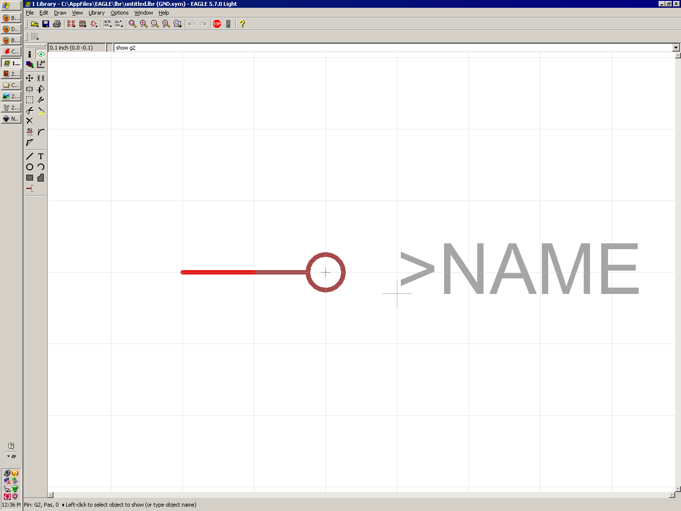
Adding symbol GND to F09-S would exceed the minimum number of pads (11) availble in package variant V


This is a device I copied directly from Eagle 5.7.0's library (con-subd.lbr) because in my design only one of the two shield lugs were being wired. I was only conecting to 10/11 pads, but adding annother GND symbol increasing the symbol count to 11 actually exceeded the pad limit of 11.


The connect window shows that there are infact 11 pins already defined, including G1 and G2. Typing show G1 in the command line is unsuccessful, therefore these pins must be defined within a symbol.


A look at the symbol (GND.sym) appears to illustrate a single pin, right clicking and selecting properties reveals G1, a wire and a circle. G2 must be nearby, and show G2 in the command line reveals that it is hidden under G1, backwards!


So in the schematic editor by using the wire tool and clicking on the GND symbol only the top pin was engaged. Had I run Eagle's Electrical Rule Check it would have produced a warning that would have confused me and prompted the same response.


The workaround:

This is a common symbol in Eagle's library, let's hope that 5.9.0 has it documented.

EDIT: typo, G2 and G1 transposed.

2010-05-31

Connecting

After I wrote that last post about my being unable to connect my brother found the new modem outside. The technician that sent it the day before said
[...] How long have you had this problem? Lets look at you router's status-* Holy-Shit! How are you even able to connect? [...] Your modem is dying, there have been more than 200000 ATM Cell Header Errors in the last two hours! [...]
and decided to send a replacement overnight express. The courier instead of putting it in the locker box or ringing the bell decided to leave it balanced on my doorstep with the "Signature Required" label face up. The courier’s website says it arrived at 1:10 PM. :|

When I installed it in the exact same place the old one was I found that while it worked considerably better than the old one, it still did not connect for more than a few minutes and about the time it racked up 10k errors I decided to try connecting it in another room. There it worked brilliantly, only one error in the first ten minutes. Thinking back to the technician's questions about what might be connected to that socket, and the knowledge that I'd in the month prior had to dig a shorting electrical recepticle out of the wall that had been plastered inplace decided to replace that socket in the first room. Now it works and picking up a phone (wired or wireless) doesn't fast-resync the DSL line.

Thinking about it now, I also recall that the cable box was secured to the electrical meter by means of framing screws, I wonder if this is the source of the phantom rings that have been annoying us during the day. I will need to make a meter long insulated screwdriver and remove them. It can't have been legal to drive metal spikes into the meter the first place.

2010-05-21

unable to connect.

Another DSL modem has failed and I am now waiting for a replacement.

My connections have been deteriorating since the meter guy had a tantrum and tore the phone and cable boxes off of the wall two years ago. I strongly suspect that the 'contractor' they sent out to fix it wired something into my loop that should not be there since
  1. the boxes are now supported by their wires
  2. there are wire splices outside of the box
  3. my digital cable is fed through the phone box
  4. there are loose fasteners inside the sealed boxes
  5. and
  6. without exaggeration, I can throw a rock and hit the CO across the intersection from my house and yet my signal quality swings from nil to excellent every few mintues


As a subscriber to both Bell and Rodgers I am understandably disappointed;
when I travel south into Toronto for work I am not excited to be meeting in person with my peers but able to get their e-mail.

If only my mother wasn't javascript:void(0)determined to keep her Bell e-mail address, then we could switch to a better DSL vendor (who would actually be selling us Bell internet, but at a better price and) with technicians who would understand that a loop that has toased three modems probabaly has something wrong in it.

2010-04-15

Yeah!

The project I mentioned eariler on this blog in Aww Fuck, has finished its initial design phase and is about due to begin prototyping.

It is a developer board w/ perpherials (serial, GPIF, ADC, bellswhistles, etc.) based on the Digikey.com:Cypress EZ-USB FX2LP™, successor to the Cypress EZ-USB FX™ which my team built the Turner oscilloscope with.[1]

In contrast to the $500 Digikey.com:Cypress EZ-USB Development Kit this has been designed down to a minimum system with only the peripherials needed to use the Microprocessor. I won't promise an exact price, but i expect that it will sell for less than $100 and more than $20.

I plan to develop a number of projects with this board over the next year, including the keyboard.

2010-04-10

Rubik's Cube continued

About two weeks ago I came up with a workable design, and key layout for this thing.

I had to make it a 3x3 (2-1-2) so that the electrical interconnects with the corner pieces not be interrupted by turning the faces without building a tree of phonojacks, or having to make extremely precise overlaping cone shaped cuts into a solid base material, then inlaying wires and springs to establish the same connections.

This is also good since I can also getaway with lower build quality.

I had hoped to use this as an exercise to learn sourceforge.net:KyCAD, however the design I have come up with makes use of concentric rings to match the connectors I have designed which has made this too difficult for me to implement on my first day using KyCAD.

So I went back to Eagle to draw the inner faces of the cubes, and after learning that it would cost me $40 for enough DigiKey:tactile switches I will be building my own switches.

If this works I promise to make a this into a kit.

XD , I can implmplement the W3Schools.com:ISO 8859-1 Symbols on the extra 30 (odd) empty cells! No more will I need to remember
Alt
+{
1
,
8
,
1
}=µ or
Alt
+{
9
,
3
,
7
}=Ω